Smart Kitchen
Flood, Smoke and Fire Hazards Protection.

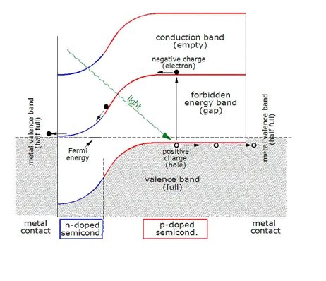
Photovoltaic Panels and Solar Cells play a pivotal role in harnessing solar energy and converting it into electricity. Over the years, advancements in materials and technology have revolutionized the efficiency, durability, and affordability of solar cells, making them a key player in the transition toward a cleaner and greener future.
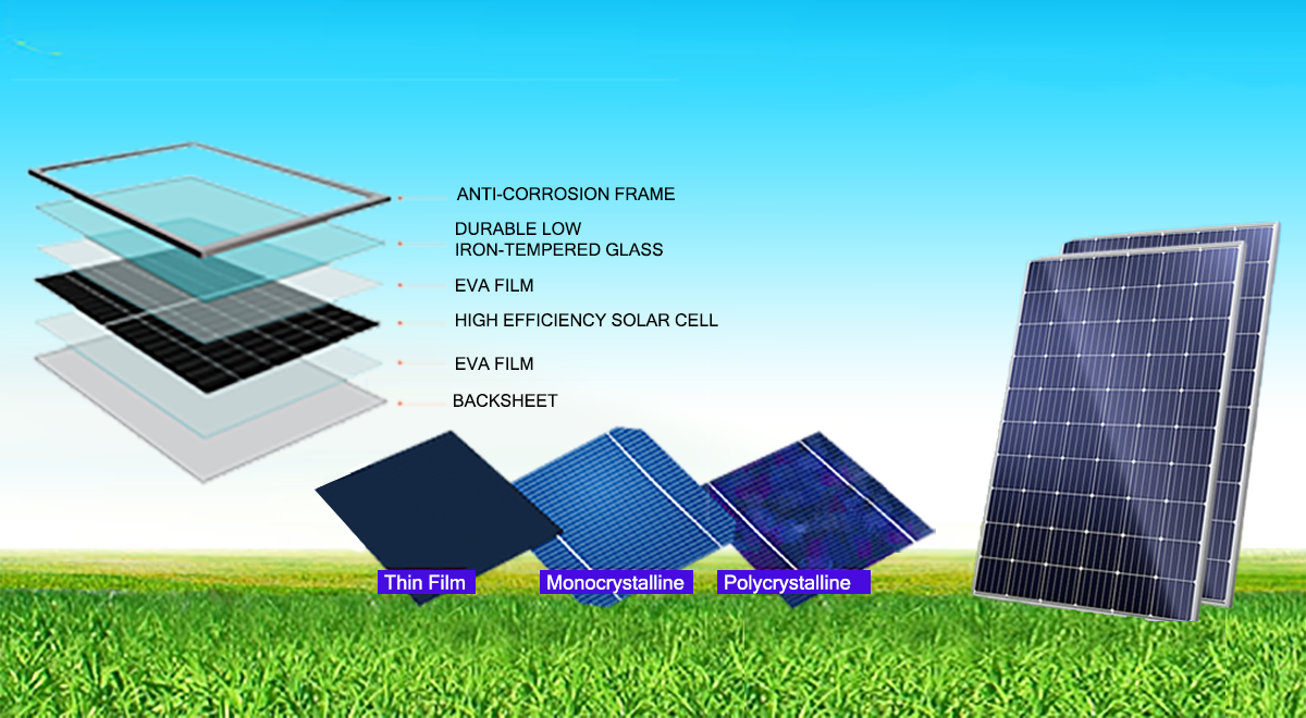
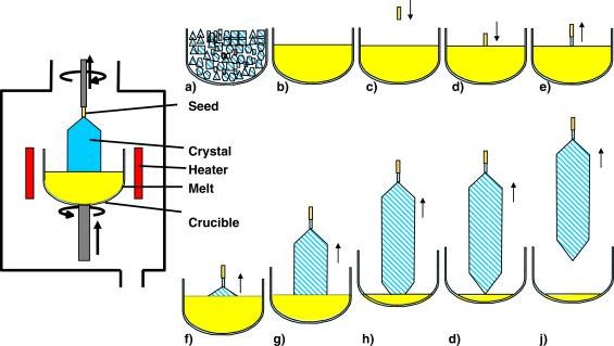
Fig.2 (a). Mono-Si growth by the Czochralski method.
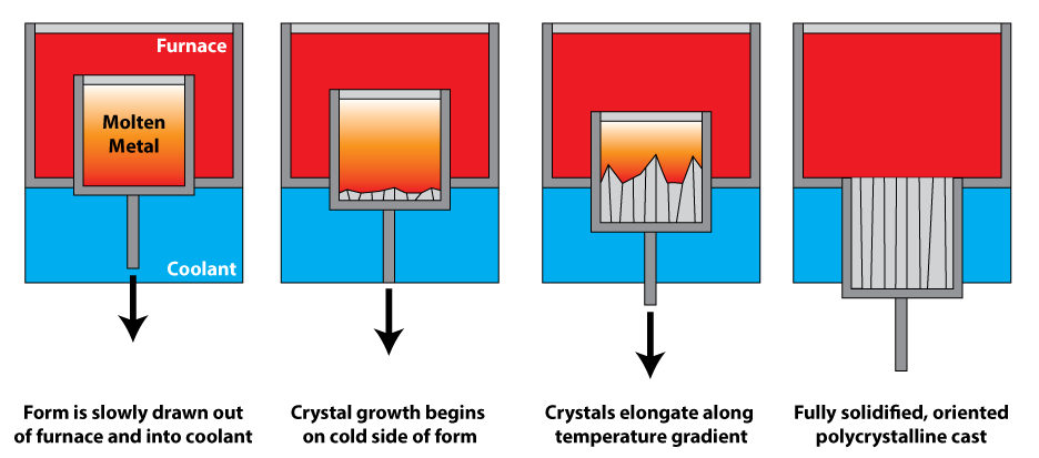
Fig.2 (b). Poly-Si casting by Directional Solidification.
Fig. 2(c) Illustrates the main steps involved in manufacturing PV panels from the raw Silicon material involving the two methods shown above.
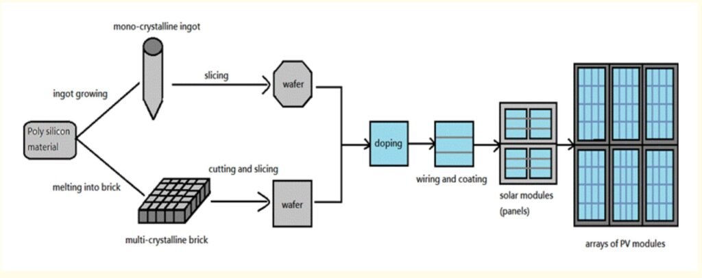
Fig.2 (c). Main steps from row Si to PV panels.
In our discussion of cutting-edge solar cell technologies, we will also explore other materials such as CdTe and Perovskite, which have their optical Bandgap optimized to harness the solar light spectrum effectively.
Back surface field (BSF) consists of creating a high-low junction, i.e. p-p+ or n-n+ at the rear side of the solar cell (depending on the doping type of the substrate) that builds a field-effect passivation (Fig. 3). For industrial standard screen–printed p-type Si solar cells, the state-of-the-art rear side passivation is realized by the p-p+ junction using aluminum BSF. The aluminum BSF is optimized for industrial solar cells since it provides good contact, field-effect passivation, and reflection on the rear side in a very simple step. For high-efficiency Si solar cells, the Al BSF is partially used such as the implementation of a passivated rear with local Al BSF (PERC-type solar cell).
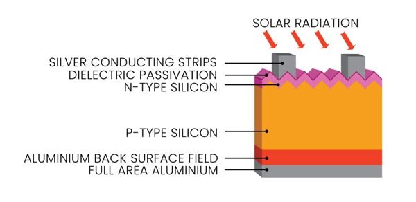
Fig.3. Aluminum Back Surface Filed Si Solar Cell.
The PERC solar cell technology includes dielectric surface passivation that reduces electron surface recombination (Fig. 4). At the same time, the PERC solar cell reduces the semiconductor-metal area of contact and increases the rear surface reflection by including a dielectrically displaced rear metal reflector. This allows photons to be absorbed when going into the cell or out of it, and it also reduces heat absorption.
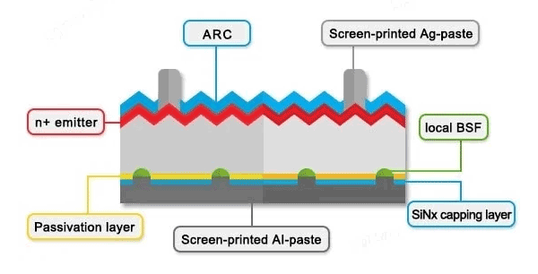
Fig.4. PERC Solar Cell structure.
Tunnel oxide passivated contact (TOPCon) solar cell technology is a new development with the potential to replace passivated emitter and rear contact (PERC) solar panels. The TOPCon solar cells are manufactured with an n-type crystalline silicon (c-Si) bulk layer because of its higher surface quality and it is coupled with a p+ emitter layer to create the p-n junction (Fig. 5).
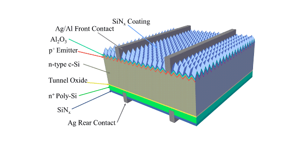
Fig.5. TOPCon Solar Cell structure.
Interdigitated Back Contact (IBC) solar cell technology is one of the most innovative methods to have proven higher efficiencies using crystalline silicon (c-Si) cells. IBC technology surpasses PERC technology in its efficiency (26.7% vs 24.3%), but comes at a slightly higher price. The core component in the IBC solar cell is the n-type crystalline silicon (c-Si) wafer functioning as the absorbing layer (Fig. 6). Subsequently, an anti-reflective and passivation layer, often composed of SiO2, is applied to one or both sides of the solar cell.
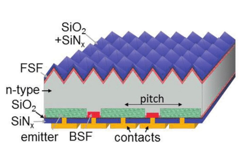
Fig.6. IBC Solar Cell Structure.
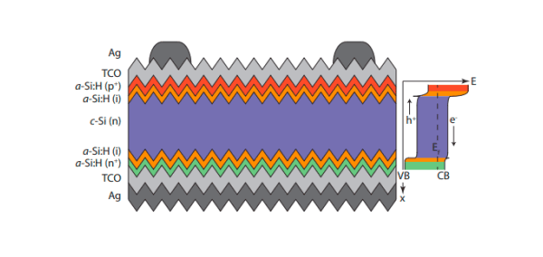
Fig.7. HJT Solar Cell Structure.
The absorber component within the heterojunction solar cell encompasses a layer based on c-Si wafer (Fig. 7 indicated in blue). This c-Si layer is sandwiched between two thin intrinsic (i) a-Si:H layers (depicted in yellow), while doped a-Si:H layers (colored in red and green) are positioned atop each respective a-Si:H (i) layer. The number of Transparent Conductive Oxide (TCO) layers depends on whether the HJT cell is monofacial or bifacial. In monofacial heterojunction cells, the backmost layer is a metal layer, serving as the conductor. During the light-absorption process, the initial photons that arrive are absorbed by the outermost a-Si:H layer, resulting in their conversion into electricity. The bulk of the incoming photons, however, undergo conversion within the c-Si layer, which boasts the highest solar conversion efficiency among the various materials within the cell. Eventually, the remaining photons reach the rear a-Si:H layer of the module, where they are ultimately transformed into electricity. This stepwise sequence ensures the high efficiency of up to 26.7% of monofacial HJT solar cells.
A Bifacial solar cell is one of the newest solar power innovations. It functions as a dual-sided energy generator, converting sunlight into electrical energy on both its upper and lower surfaces. The term “bifacial” originates from “bi-” (meaning two) and “facial” (pertaining to the face). Bifacial photovoltaic panels and solar cells are designed with solar cells on both the upper and rear sides of the structure (Fig. 8). The front captures incident sunlight while the back absorbs reflected light. More captured sunlight means greater solar cell efficiency compared with traditional solar cells.
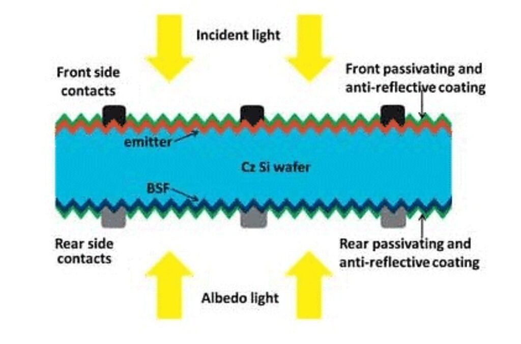
Fig.8. Bifacial Solar Cell Structure.
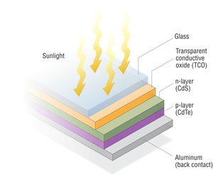
Fig.9. CdTe Thin Film Solar Cell Structure.
The most common CdTe solar cells (Fig. 9) consist of a p-n heterojunction structure containing a p-doped CdTe layer matched with an n-doped cadmium sulfide (CdS) or magnesium zinc oxide (MZO) window layer. Typical CdTe thin-film deposition techniques include vapor-transport deposition and close-spaced sublimation. CdTe absorber layers are generally grown on top of a high-quality transparent conductive oxide (TCO) layer—usually fluorine-doped tin oxide (SnO2:F). Cells are completed using a back electrical contact—typically a layer of zinc telluride (ZnTe) followed by a metal layer or a carbon paste that also introduces copper (Cu) into the rear of the cell.
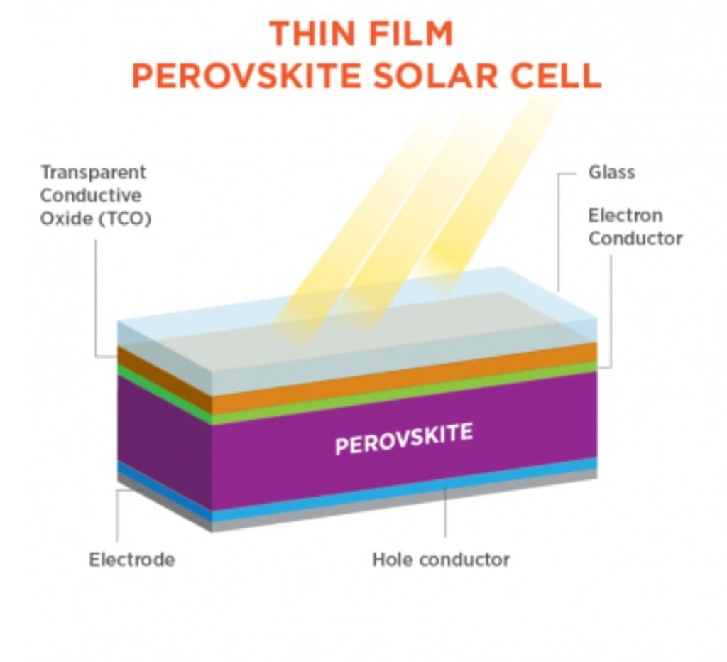
Fig.10. Perovskite Thin Film Solar Cell Structure.
The most common Perovskite thin film solar cells (Fig. 10) consist of a Perovskite flat layer sandwiched between n-type (Electron conductor) and p-type (Hole conductor) layers. After light absorption, both charge generation, as well as charge extraction, occur in the Perovskite layer.
Perovskites exhibit the capacity to be adjusted in response to distinct colors across the solar spectrum through alterations in material composition. Various formulations have showcased impressive performance levels. This adaptability permits the pairing of perovskites with divergent absorber materials, yielding increased power output from the same device. This configuration is termed a tandem device architecture (Fig. 11). By incorporating multiple photovoltaic materials, tandem devices can potentially achieve power conversion efficiencies exceeding 33%, surpassing the theoretical cap of a single junction PV cell.
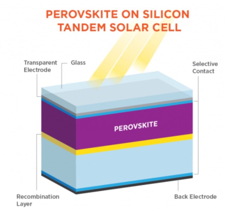
Fig.11. Perovskite on Silicon Tandem Solar Cell Structure.
In conclusion, by optimizing light absorption, charge carrier generation, and carrier collection, solar cells can achieve higher efficiency while keeping manufacturing costs down. These advancements play a crucial role in harnessing solar energy more effectively and sustainably.
Solar photovoltaic (PV) panels vary in type and size based on their composition (mono-crystalline, polycrystalline, thin film) and solar cell structures (PERC, TOPCon, IBC, HJT, thin film CdTe, or Perovskite). In addition, these panels need to meet specific criteria for optimal functionality, including maximizing power output, reliability during varying weather conditions that could cause shading or damage, and even aesthetic considerations. As a result, distinct panel categories have emerged to address these specific requirements, which we’ll discuss here.
Half-cut cell panels provide several benefits over traditional solar cells. Most important of them are increased partial shading tolerance and reduced resistivity losses. Performance-wise, half-cut cells can increase panel efficiencies by a few percentage points. Generally, modules with 60 solar cells include three substrings of 20 cells in series (Fig. 12). The equivalent half-cut solar cell modules have 120 solar cells, divided into six substrings of 20 cells. Each side of the half-cut solar panel has three substrings in parallel, with both sides also connected in parallel.
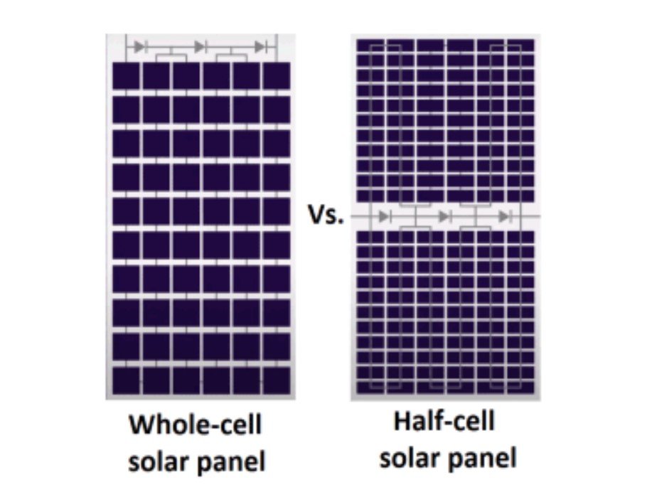
Fig.12. Half-Cut Solar PV Panels vs Standard PV Panels.
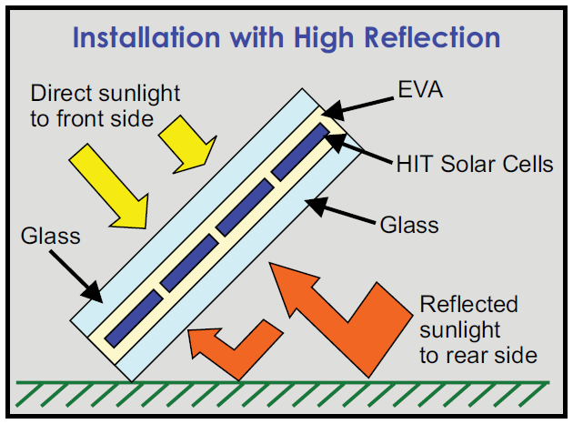
Fig. 13a. Angled Installation of Bifacial Solar PV Panel.
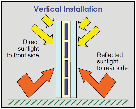
Fig. 13b. Vertical Installation of Bifacial Solar PV Panel.
In contrast to monofacial solar panels, which are typically positioned parallel to surfaces like rooftops, bifacial panels exhibit higher energy output when angled away from the roof or ground at varying degrees (Fig. 13a). In such tilted setups, considerable reflection takes place. Bifacial solar panels excel at capturing sunlight from diverse angles, as sunlight reflects off objects at numerous angles. This attribute empowers them to perform effectively even on overcast days, a scenario where monofacial solar cells face greater limitations. An alternative installation approach involves placing bifacial panels vertically (Fig. 13b), resulting in two energy production peaks each day.
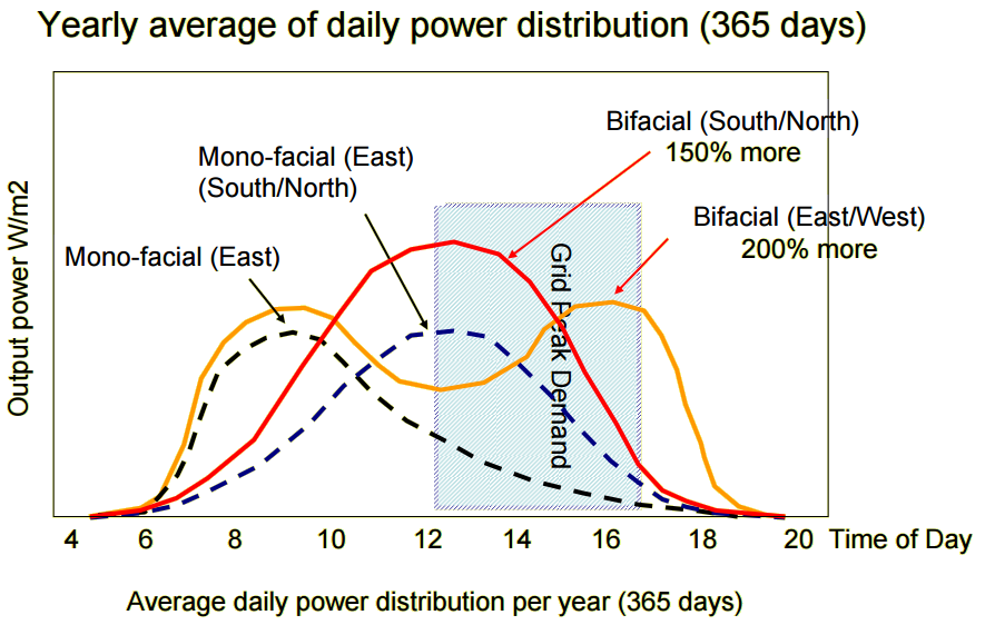
Fig. 13c. Bifacial Solar PV Panel’s Daily Power Distribution.
During these peaks, sunlight’s reflection on the opposite side of the panels further contributes to energy generation (Fig. 13c). Notably, vertical setups are less susceptible to obstruction by snow or blown sand during inclement weather. Bifacial solar panels stand out due to their dual glass covers, which enhance their durability compared to conventional solar panel systems. Consequently, warranties for bifacial panels often extend for more than 5 years beyond those of conventional panels, providing a lifespan of 30+ years as opposed to the typical 20–25 years. Some of the leading Bifacial Solar PV Panels manufacturers today are Trina, REC Solar, Canadian Solar, Longi, Jinko, and others.
All-Black Solar PV Panels‘ biggest advantage is the aesthetic (Fig. 14). Traditional panels use white backsheets and silver frames, while All-Black modules use black backsheets and black frames. They’re manufactured the same way through the same processes, except black adhesives may be used around junction boxes and other electronics on All-Black modules. The major difference between the two is their efficiency ratings. All-Black modules run a bit hotter and offer fewer opportunities for reflected light absorption, so their efficiencies are about 0.5% lower.
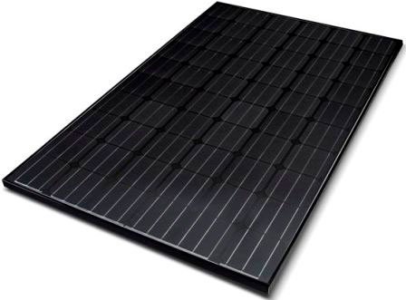
Fig. 14. All-Black Solar PV Panel.
Cadmium Telluride (CdTe) -based solar PV Panels have taken the forefront as the predominant commercially adopted thin film photovoltaic technology (Fig. 15a). They inherently exhibit superior temperature coefficients, energy yield, and degradation rates when compared to silicon (Si) technologies.
Fig. 15a. CdTe Thin-Film Solar PV Panel.
The prevailing technology for CdTe-based modules presently centers around a thin film absorber layer of p-type doped CdTe or graded CdSe1-xTex (CdSeTe) (Fig. 15b). These polycrystalline layers possess a minimal bandgap, approximately 1.5 eV for CdTe and ∼1.4 eV for CdSeTe, respectively. These absorber layers are produced in a superstrate arrangement, situated on glass to allow light to pass through. To ensure enduring reliability and reduced degradation in most commercial modules, an additional sheet of glass and edge seals are used to hermetically encase the module. This configuration presents a significant opportunity for the development of bifacial modules featuring transparent back electrodes.
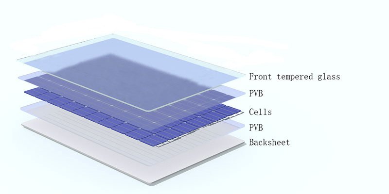
Fig. 15b. CdTe Thin-Film Solar PV Panel Structure.